





Global Silicon Carbide Wafer Processing Equipment Market Research Report 2026 (Status and Outlook)
Silicon carbide wafer processing equipment refers to the specialised manufacturing systems used to process SiC substrates and wafers through semiconductor production. These tools are designed to handle the extreme hardness, brittleness and thermal stability of silicon carbide, a wide-bandgap semiconductor material widely adopted in high-power and high-frequency electronics. Compared with conventional silicon wafer equipment, SiC processing systems require higher precision, stronger wear resistance and tighter process control because the material’s unique physical characteristics dictate every downstream step. The equipment portfolio typically covers crystal slicing, grinding, lapping, polishing, cleaning, epitaxy preparation, inspection and wafer handling. As the semiconductor industry shifts toward electric vehicles, renewable energy systems, industrial automation and advanced power electronics, demand for high-yield SiC wafer processing equipment continues to re-accelerate from the 2025 trough.
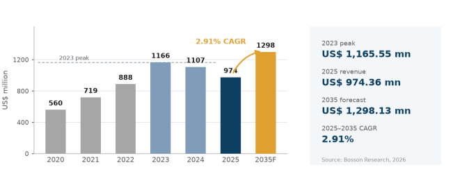
In 2025, the global SiC wafer processing equipment market stood at US$ 974.36 million, down from a peak of US$ 1,165.55 million in 2023, and is forecast to expand at a 2.91% CAGR between 2026 and 2035 to reach US$ 1,298.13 million. The trajectory is unusual because the market is emerging from a capacity correction rather than an expansion: the unprecedented capital expenditure wave of 2019–2024 built substrate and epitaxy capacity ahead of demand, and 2025 utilisation of roughly 50% in upstream processes reflects that overhang. Growth is driven by the transition from 6-inch to 8-inch wafer diameters, which forces retooling of the entire process flow, and by 800V electric vehicle platforms, AI data centre power delivery and advanced packaging.
However, despite its long-term potential, the SiC wafer processing equipment market faces significant challenges across capacity, price and trade. Substrate and epitaxy utilisation fell to approximately 50% in 2025 while device lines ran at around 70%, and the average price of 6-inch SiC substrates dropped approximately 40% year-on-year in the first quarter of 2025, which propagates backward into equipment order books. The commercialisation timelines of emerging applications including AI data centres and solid-state transformers remain highly uncertain. US export controls on semiconductor equipment continue to expand, and the physical limits of processing a material with a Mohs hardness near 9.5 remain unsolved.
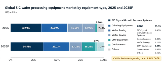
By equipment type, six families span the value chain, from crystal growth furnaces operating above 2,000°C to precision polishing tools holding surfaces to angstrom-level roughness. SiC crystal growth furnace systems accounted for 32.94% of 2025 revenue and grinding equipment for 29.09%, giving the two front-end tools a combined 62.03% share. CMP equipment, at 13.95%, is the fastest-growing category at a 3.84% CAGR through 2035, because epitaxial growth and device fabrication remain unforgiving of surface defects. Wafer sawing, at 15.65%, grows at just 1.21% and goniometers at 1.43%. By 2035 growth furnace systems are forecast to hold 34.53% of global revenue and CMP to expand to 15.26%.
Table 1 Global SiC wafer processing equipment market by product type, 2025 and 2035F (US$ million)
|
Equipment type |
2025 |
2035F |
Share 2025 |
Share 2035F |
CAGR 25-35 |
|---|---|---|---|---|---|
|
SiC Crystal Growth Furnace Systems |
320.93 |
448.30 |
32.94% |
34.53% |
3.40% |
|
Grinding Equipment |
283.48 |
376.81 |
29.09% |
29.03% |
2.89% |
|
Wafer Sawing |
152.49 |
171.95 |
15.65% |
13.25% |
1.21% |
|
CMP Equipment |
135.88 |
198.15 |
13.95% |
15.26% |
3.84% |
|
Goniometers |
8.72 |
10.06 |
0.90% |
0.77% |
1.43% |
|
Others |
72.84 |
92.86 |
7.48% |
7.15% |
2.46% |
|
Total |
974.36 |
1,298.13 |
100.00% |
100.00% |
2.91% |
Source: Bosson Research analysis, 2026.
From an application perspective, power devices dominate and stay dominated. Power device manufacturing accounted for 79.47% of 2025 revenue and reaches 80.80% by 2035 on a 3.08% CAGR, spanning SiC MOSFETs, Schottky diodes and power modules used in electric vehicles, renewable energy systems, industrial motor drives and fast-charging infrastructure. SiC enables higher switching frequency, lower energy loss and improved thermal performance compared with silicon, which makes it ideal for high-power environments. Electronics and optoelectronics hold 11.43% and wireless infrastructure 3.82%, with AR glasses waveguides emerging as a new consumer electronics pocket.
Table 2 Global SiC wafer processing equipment market by application, 2025 and 2035F (US$ million)
|
Application |
2025 |
2035F |
Share 2025 |
Share 2035F |
CAGR 25-35 |
|---|---|---|---|---|---|
|
Power Device |
774.34 |
1,048.95 |
79.47% |
80.80% |
3.08% |
|
Electronics and Optoelectronics |
111.40 |
142.39 |
11.43% |
10.97% |
2.48% |
|
Others |
51.41 |
61.02 |
5.28% |
4.70% |
1.73% |
|
Wireless Infrastructure |
37.20 |
45.76 |
3.82% |
3.53% |
2.09% |
|
Total |
974.36 |
1,298.13 |
100.00% |
100.00% |
2.91% |
Source: Bosson Research analysis, 2026.

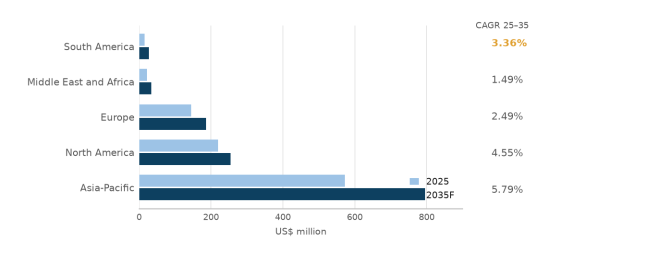
Geographically, the market is heavily concentrated in Asia-Pacific, which held 58.69% of 2025 revenue and 63.57% of units shipped. China alone accounts for 42.96% of global revenue and 64.89% of units shipped, with Chinese companies holding approximately 40% of global SiC wafer and epitaxial wafer capacity by 2024. North America is second at 22.56% and Europe third at 14.90%. The growth profile diverges from the revenue ranking: South America grows fastest at a 5.79% CAGR and Middle East and Africa at 4.55%, while North America lags at 1.49% because its installed base is mature and its fab additions are concentrated in leading-edge logic rather than SiC. Within Asia-Pacific, Japan grew revenue to US$ 247.92 million in 2025, overtaking Europe, while China saw revenue fall from its 2023 peak of US$ 580.18 million to US$ 418.55 million.
Table 3 Global SiC wafer processing equipment market by region, 2025 and 2035F (US$ million)
|
Region |
2025 |
2035F |
Share 2025 |
CAGR 25-35 |
|---|---|---|---|---|
|
Asia-Pacific |
571.81 |
795.86 |
58.69% |
3.36% |
|
North America |
219.83 |
254.98 |
22.56% |
1.49% |
|
Europe |
145.14 |
185.62 |
14.90% |
2.49% |
|
Middle East and Africa |
21.95 |
34.24 |
2.25% |
4.55% |
|
South America |
15.63 |
27.43 |
1.60% |
5.79% |
|
Total |
974.36 |
1,298.13 |
100.00% |
2.91% |
Source: Bosson Research analysis, 2026.
Silicon Carbide Wafer Processing Equipment Industry Chain Analysis

Manufacturing Process Analysis of SiC Wafer Processing Equipment
Crystal Growth Furnace Systems
SiC crystal growth furnace systems are the core upstream equipment used to produce high-quality silicon carbide boules through physical vapour transport or modified sublimation methods. These furnaces operate at temperatures above 2,000°C and require precise thermal field control to manage crystal defect density, polytype stability and growth rate. The equipment is highly complex, involving advanced temperature zoning, vacuum control and seed crystal positioning systems. Performance directly determines wafer quality, yield and downstream device reliability, making it the most strategically critical segment in the SiC value chain. The segment is characterised by high capital intensity, long development cycles and strong technological barriers.
The thermal field system acts as the heart of the furnace, combining graphite crucibles, heaters, flow-guiding rings and insulation materials such as graphite soft and hard felt. Operating above 2,400°C, it establishes a precise axial temperature gradient of 5–15°C/cm that drives vapour-phase species toward the seed crystal and crystallises them. The purity, uniformity and lifetime of these materials directly affect defect density and yield. Crucibles and insulation are high-frequency consumables, typically replaced every one to two months and three to four months respectively, so the installed base generates a recurring consumables stream independent of new furnace sales.
Heating and atmosphere control complete the system. Power and heating rely on medium- to high-frequency induction at 2–20 kHz, converting electrical energy into heat through induction coils that precisely heat the graphite crucible; accurate frequency control adjusts magnetic field penetration depth and carries a very high technical barrier. In the thermal field segment, global leader SGL Carbon provides the full range of heaters, crucibles and graphite insulation cylinders, while high-frequency stability is the province of international suppliers such as TRUMPF. Dry vacuum pump suppliers include the Institute of Microelectronics of the Chinese Academy of Sciences and other specialists.
CMP is the hardest of the three because silicon carbide resists both mechanical abrasion and chemical etching. It requires specialised slurry formulations and high-pressure polishing heads, and it runs as a multi-step process of rough polishing, fine polishing and final surface finishing. Consumable dependency is heavy on pads and slurries, roughness control is held to angstrom-level requirements, and process integration complexity is the highest of any segment. CMP is essential for enabling high-performance epitaxial growth and device fabrication, which is why it is also the fastest-growing category at a 3.84% CAGR even from a 13.95% revenue share.
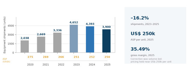
Equipment shipments and revenue contracted in near lockstep. Shipments peaked at 4,652 units in 2023 and fell to 3,900 in 2025, a 16.2% decline, while revenue over the same period fell 16.4% to US$ 974.36 million. Average pricing has been remarkably stable, moving from US$ 251 thousand per unit in 2023 to US$ 250 thousand in 2025, which means the correction has been a volume phenomenon rather than a price collapse at the equipment layer. Gross margin held at 35.49% in 2025 against 35.51% in 2023, and the 2020–2025 average price has drifted only from US$ 275 thousand to US$ 250 thousand per unit.
Table 4 Global SiC wafer processing equipment shipments, pricing and margin, 2020-2025
|
Metric |
2020 |
2021 |
2022 |
2023 |
2024 |
2025 |
|---|---|---|---|---|---|---|
|
Equipment shipments (units) |
2,038 |
2,669 |
3,336 |
4,652 |
4,393 |
3,900 |
|
Revenue (US$ million) |
559.70 |
719.02 |
887.74 |
1,165.55 |
1,106.95 |
974.36 |
|
Average price (US$ thousand/unit) |
275 |
269 |
266 |
251 |
252 |
250 |
|
Gross margin |
33.99% |
35.32% |
34.83% |
35.51% |
35.30% |
35.49% |
Source: Bosson Research analysis, 2026.
Grinding, Sawing and CMP Processing
Grinding equipment shapes and thins SiC wafers after slicing, removing subsurface damage and reaching target thickness and flatness before polishing. Given the material’s extreme hardness, grinding systems require ultra-rigid machine structures, high-speed spindles and diamond abrasives, and they are increasingly integrated with in-situ metrology and automation to lift yield and reduce the downstream CMP burden. Wafer sawing slices SiC ingots using diamond wire or laser-based cutting technologies; at a Mohs hardness near 9.5, conventional slicing is ineffective, so diamond wire sawing dominates. Tool wear rates are high, surface damage control is stringent and kerf loss reduction directly moves wafer cost structure.
Development Trends
Capacity Correction Has Reset the Market, and the Recovery Is Now Shaped by Wafer Size
The single most important fact about this market is that it is coming out of a capacity cycle rather than entering one. Between 2019 and 2024 the SiC industry went through its first major capital expenditure wave, described by Yole Group as unprecedented. Substrate and epitaxy capacity was built ahead of demand, and the consequence is visible in the equipment numbers: a peak of 4,652 units shipped in 2023 against 3,900 in 2025. Chinese companies accounted for approximately 40% of global SiC wafer and epitaxial wafer capacity by 2024, and most incremental equipment investment has been concentrated in mainland China.
That correction has now worked through the value chain. In 2025, capacity utilisation for upstream substrate and epitaxy processes fell to approximately 50%, while device production lines operated at around 70%. Equipment makers have absorbed the consequence in their order books, and the market is forecast to grow from that lower base rather than from the 2023 peak. Revenue reaches US$ 1,298.13 million by 2035 — above the 2023 peak, but reached six years later and with a lower unit count than the 2023 peak implied.
The forward-looking variable is wafer diameter. The transition from 6-inch to 8-inch substrates, and eventually to 12-inch, represents the most significant technology trend in the industry and the most important technology-driven growth opportunity for the equipment market. Wolfspeed launched its 200mm SiC platform as the leading indicator of that shift. Because larger wafers change the tooling mix entirely — a different number of growth furnaces and different grinding and CMP configurations per line — the diameter shift is what converts a flat unit market into a value-growth market, and it is why CMP grows faster than the market average.
Against this backdrop, silicon carbide wafer processing equipment have emerged as an “upgraded biomass fuel.” Through torrefaction, they significantly enhance energy density, improve hydrophobicity, and increase grindability, making them more coal-like and enabling lower-cost integration into existing coal-fired systems. This “substitute upgrade” logic forms the most fundamental and certain growth driver of the silicon carbide wafer processing equipment market. Currently, the market is transitioning from early-stage technical validation and demonstration projects to large-scale commercialization. A key indicator of this shift is that major energy companies are signing long-term supply agreements and promoting upstream capacity construction, meaning market demand is no longer scattered pilot projects but predictable and sustainable procurement behavior.
Growth Furnace Systems Dominate, CMP Is the Fastest-Growing Segment
Equipment demand divides into two commercial camps. Growth furnace systems, at 32.94% of 2025 revenue, remain the anchor: they are the largest single capital outlay in a SiC fab and the segment with the highest technological barrier, combining thermal field design, vacuum control and polytype stability. Grinding, at 29.09%, is the second pillar and the more mature of the two in terms of process know-how. The moat in growth furnaces is thermal field engineering accumulated over many generations, not a single patent.
CMP occupies the growth position. Small at 13.95% of 2025 revenue, it compounds at 3.84% through 2035, outpacing the 2.91% market average, because every device generation tightens the surface specification that CMP delivers and because the epitaxial step that follows is far less forgiving of residual damage than the grinding step that precedes it. Goniometers, at 0.90%, are metrology whose value sits in process control rather than throughput, and the fragmented "others" category, at 7.48%, covers edge rounding, cleaning, inspection and lapping tools.
A third front is opening in high-throughput epitaxy preparation. As wafer diameters move up, the number of growth furnaces required per unit of output falls but their individual capacity rises, which favours larger, more automated systems with tighter thermal uniformity. This is where incumbents with long-standing materials and vacuum partnerships retain a defensible position, and where the next round of consumable development is concentrated.
Driving Factors
Wafer Size Transition and EV Platforms
The core driver of the SiC wafer processing equipment market is the transition in wafer diameter, not end-market unit growth. Moving from 6-inch to 8-inch substrates requires retooling an entirely different process flow, and because each diameter generation arrives with new process recipes and tighter specifications, equipment demand re-accelerates even when wafer output does not. The same logic applies to the cutting technology generation shift, where laser-based methods are displacing conventional diamond wire where kerf loss dominates.
Electric vehicles amplify the effect. SiC MOSFETs are increasingly adopted across 800V high-voltage platforms, where the device must handle high switching frequencies with low conduction loss, and where every additional vehicle platform multiplies demand for high-quality substrates and therefore for the equipment that makes them. AI data centres are emerging as a second growth curve, with rack-level power density pushing SiC into power delivery architectures.
Cost pressure pulls in the other direction. In the first quarter of 2025 the average price of 6-inch SiC substrates fell by approximately 40% year-on-year, and that pressure propagates backward into equipment orders. Vendors that cannot demonstrate yield improvement per unit of installed capacity face order deferral even as the long-run market grows. This is the reason gross margin in standard grinding and sawing equipment is structurally thinner than in growth furnace systems, where consumables and process know-how create stickier economics.
Localisation Policy and Capacity Building
Semiconductor localisation is the second structural driver, and it is largely a China story. Chinese companies accounted for approximately 40% of global SiC wafer and epitaxial wafer capacity by 2024, and domestic Chinese equipment vendors now occupy five of the top nine positions in 2025 revenue. Support takes several forms: state-backed capacity programmes, local content requirements in funded projects and direct financing for wafer and equipment capacity.
The concentration figures show how open the field remains. The five largest vendors held 37.76% of 2025 revenue, down from 40.38% in 2023, and the Herfindahl-Hirschman Index stands at 2.93% — a highly fragmented structure in which no single vendor holds more than 9%. NAURA Technology Group leads with US$ 87.40 million, Zhejiang Jingsheng at US$ 86.05 million and Beijing Semicore at US$ 72.51 million, with Applied Materials the highest-ranked non-Chinese player at US$ 68.63 million.
On the supply side, export controls cut both ways. They constrain access to the most advanced metrology and materials for Chinese suppliers, but they also guarantee a protected domestic market large enough to fund the learning curve — the same dynamic that played out in lithography-adjacent equipment over the past decade. SEMI has identified semiconductor equipment as a focus of US trade restriction, and the SiC supply chain is increasingly affected.
Technological Advancement
Process Technology, Consumables and Yield
The third driver is the material itself. Silicon carbide has a Mohs hardness of approximately 9.5, second only to diamond, and its extreme hardness and brittleness create fundamental difficulty throughout the wafer processing stage. Yield loss from subsurface microcracks, edge chipping and residual surface damage sets a ceiling on how cheap processed SiC can become, and therefore on how much equipment investment the value chain can support.
Process innovation is the enabling answer. In-situ metrology integration into grinding reduces the downstream CMP burden; multi-step polishing with dedicated slurry chemistry addresses the chemical inertness of the material; and laser-based cutting is displacing conventional sawing where kerf loss dominates material cost. Each of these is a multi-year qualification in its own right, which is why the supplier base at the premium end has changed so little.
Material innovation is advancing in parallel. Graphite thermal field components, high-purity quartz and advanced diamond abrasives determine throughput and defect density in growth and grinding, and supplier concentration in these consumables is a meaningful lever on cost of ownership for equipment buyers. Consumable replacement cycles — one to two months for crucibles, three to four months for insulation — mean the installed base keeps paying into the supply chain long after the original equipment sale.
Global Silicon Carbide Wafer Processing Equipment Market: Competitive Landscape
The global SiC wafer processing equipment sector is concentrated but not locked. The five largest vendors together held 37.76% of 2025 revenue, down from 40.38% in 2023, and the Herfindahl-Hirschman Index stands at 2.93% — a highly fragmented structure in which no single vendor holds more than 9%. NAURA Technology Group leads the 2025 ranking with US$ 87.40 million, followed by Zhejiang Jingsheng Mechanical & Electrical at US$ 86.05 million and Beijing Semicore Microelectronics Equipment Co., Ltd. at US$ 72.51 million. Behind them sits a broad second tier spanning Japan, the United States and mainland China, gaining ground through consumables supply, local customer access and rapid capacity addition.

Global Silicon Carbide Wafer Processing Equipment Market: Market Segmentation Analysis
The research report includes specific segments by region (country), manufacturers, Type, and Application. Market segmentation creates subsets of a market based on product type, end-user or Application, Geographic, and other factors. By understanding the market segments, the decision-maker can leverage this targeting in the product, sales, and marketing strategies. Market segments can power your product development cycles by informing how you create product offerings for different segments.
Key Company
Zhejiang Jingsheng Mechanical & Electrical
Beijing Semicore Microelectronics Equipment Co., Ltd.
Applied Materials
Yujing Machinery
ACCRETECH
Ebara Corporation
Suzhou Uking Semiconductor Technology
Revasum
Others
SiC Crystal Growth Furnace Systems
Grinding Equipment
Wafer Sawing
Power Device
Electronics and Optoelectronics
Wireless Infrastructure
Asia-Pacific
North America
Europe
Middle East and Africa
South America
Key Benefits of This Market Research:
• Industry drivers, restraints, and opportunities covered in the study
• Neutral perspective on the market performance
• Recent industry trends and developments
• Competitive landscape & strategies of key players
• Potential & niche segments and regions exhibiting promising growth covered
• Historical, current, and projected market size, in terms of value
• In-depth analysis of the Silicon Carbide Wafer Processing Equipment Market
• Overview of the regional outlook of the SiC wafer processing equipment market
Key Reasons to Buy this Report:
• Access to date statistics compiled by our researchers. These provide you with historical and forecast data, which is analyzed to tell you why your market is set to change
• This enables you to anticipate market changes to remain ahead of your competitors
• You will be able to copy data from the Excel spreadsheet straight into your marketing plans, business presentations, or other strategic documents
• The concise analysis, clear graph, and table format will enable you to pinpoint the information you require quickly
• Provision of market value (USD Million) data for each segment and sub-segment
• Indicates the region and segment that is expected to witness the fastest growth as well as to dominate the market
• Analysis by geography highlighting the consumption of the product/service in the region as well as indicating the factors that are affecting the market within each region
• Competitive landscape which incorporates the market ranking of the major players, along with new service/product launches, partnerships, business expansions, and acquisitions in the past five years of companies profiled
• Extensive company profiles comprising of company overview, company insights, product benchmarking, and SWOT analysis for the major market players
• The current as well as the future market outlook of the industry concerning recent developments which involve growth opportunities and drivers as well as challenges and restraints of both emerging as well as developed regions
• Includes in-depth analysis of the market from various perspectives through Porter’s five forces analysis
• Provides insight into the market through Value Chain
• Market dynamics scenario, along with growth opportunities of the market in the years to come
• 6-month post-sales analyst support
Customization of the Report
In case of any queries or customization requirements, please connect with our sales team, who will ensure that your requirements are met.
Note: this report may need to undergo a final check or review and this could take about 48 hours.
Chapter Outline
Chapter 1 mainly introduces the statistical scope of the report, market division standards, and market research methods.
Chapter 2 is an executive summary of different market segments (by region, product type, application, etc), including the market size of each market segment, future development potential, and so on. It offers a high-level view of the current state of the Silicon Carbide Wafer Processing Equipment Market and its likely evolution in the short to mid-term, and long term.
Chapter 3 makes a detailed analysis of the Market’s Competitive Landscape of the market and provides the market share, capacity, output, price, latest development plan, merger, and acquisition information of the main manufacturers in the market.
Chapter 4 is the analysis of the whole market industrial chain, including the upstream and downstream of the industry, as well as Porter’s five forces analysis.
Chapter 5 introduces the latest developments of the market, the driving factors and restrictive factors of the market, the challenges and risks faced by manufacturers in the industry, and the analysis of relevant policies in the industry.
Chapter 6 provides the analysis of various market segments according to product types, covering the market size and development potential of each market segment, to help readers find the blue ocean market in different market segments.
Chapter 7 provides the analysis of various market segments according to application, covering the market size and development potential of each market segment, to help readers find the blue ocean market in different downstream markets.
Chapter 8 provides a quantitative analysis of the market size and development potential of each region and its main countries and introduces the market development, future development prospects, market space, and capacity of each country in the world.
Chapter 9 details the production of products in major countries/regions and provides the production of major countries/regions.
Chapter 10 introduces the basic situation of the main companies in the market in detail, including product sales revenue, sales volume, price, gross profit margin, product portfolio, and recent development plans.
Chapter 11 provides a quantitative analysis of the market size and development potential of each region in the next five years.
Chapter 12 provides a quantitative analysis of the market size and development potential of each market segment (product type and application) in the next five years.
Chapter 13 is the main points and conclusions of the report.
