


Global Semiconductor Advanced Packaging Research Report 2025 (Status and Outlook)

Report Overview:
According to Bosson Research, the global semiconductor advanced packaging market reached USD 44 billion in 2024, and it is expected that by 2025, the market share of advanced packaging relative to traditional packaging technologies will exceed 50%, becoming the primary driver of industry upgrades and value enhancement. The packaging and testing industry exhibits a clear foundry-oriented nature and is both capital-intensive and labor-intensive, making it prone to forming industrial clusters. Driven by semiconductor industry relocation, labor cost advantages, and tax incentives, the Asia-Pacific region has gradually developed into the core hub for global IC packaging and testing. Currently, global packaging technologies are accelerating the transition from third-stage traditional packaging represented by GSP and BGA to fourth- and fifth-stage advanced packaging represented by SiP, flip-chip (FC), and bumping technologies.
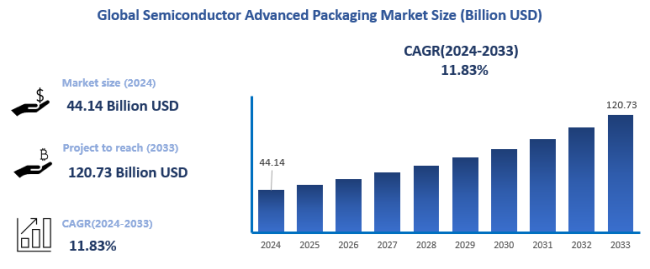
Bosson Research reports that the global semiconductor advanced packaging market is projected to expand at a compound annual growth rate (CAGR) of 11.83% from 2025 to 2033, fueled primarily by the convergence of post-Moore’s Law technical challenges and emerging application demands. As Moore’s Law slows, the benefits from process miniaturization are gradually diminishing, and bottlenecks such as the power wall, memory wall, and cost wall are becoming increasingly prominent, making it nearly impossible to further improve performance solely through wafer process scaling. Advanced packaging—through multi-chip integration, high-density interconnects, and heterogeneous packaging—enhances chip functionality and performance while reducing power consumption and optimizing costs, effectively upgrading packaging from a traditional “post-process” step to a key driver of chip performance.
Against this backdrop, global wafer fabs and OSATs are accelerating their deployment of high-end packaging, driving the value chain forward. At the same time, the exponential demand for computing power from AI large models, generative AI, and high-performance applications is further fueling the rapid expansion of the advanced packaging market, transforming it from a cost center into a value center and positioning it as a critical engine for the next phase of semiconductor industry transformation.
Market Definition and Technological Development
The AI domain is placing unprecedented challenges on the semiconductor industry. As application-end data volumes continue to expand, requirements for chip computing power, bandwidth, and energy efficiency are rising, while power consumption and thermal management issues are becoming increasingly severe. At the same time, diverse AI applications across different scenarios are driving growing demands for chip adaptability. Against this backdrop, traditional packaging technologies are struggling to meet the needs of AI chips in high-density integration, high-bandwidth transmission, and complex application scenarios.
Advanced packaging technology has therefore become a critical path for breaking the limits of Moore’s Law and achieving high-performance chip design. As Xie Jianyong, CEO of Qili Semiconductor (Shaoxing) Co., Ltd., notes, “With Moore’s Law slowing down, advanced packaging has become one of the key technological paths.” With the proliferation of innovative packaging forms such as 3D stacking, flip-chip (FC), and wafer-level packaging (WLP), advanced packaging not only provides more efficient electrical interconnects and thermal management solutions for chips but is also redefining the global semiconductor supply chain and material demand structure, creating unprecedented growth opportunities for the packaging materials market.
Semiconductor packaging refers to the interconnection methods between chips or between a chip and external circuits, with the core purpose of achieving higher performance in smaller spaces. Packaging technology has emerged alongside the invention of integrated circuits and primarily serves functions including power distribution, signal routing, thermal management, and physical protection.
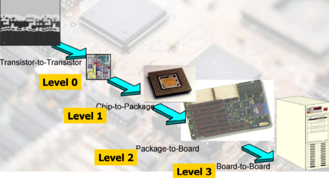
From the perspective of chips manufactured from silicon wafers, packaging can be divided into three levels. First-level packaging (single-chip module, SCM, or multi-chip module, MCM) involves encapsulating one or multiple chips into a single component. Second-level packaging (board-level packaging) integrates first-level packages with other components onto printed wiring boards (PWB) or other substrates. Third-level packaging (system-level packaging) inserts second-level packages into motherboards to form complete systems. By classification, packaging can be divided into chip-level packaging (level 0), component-level packaging (level 1), board-level packaging (level 2), and system-level packaging (level 3), with advanced packaging primarily referring to component-level packaging.
Traditional packaging generally refers to the process of cutting silicon wafers into individual chips and then encapsulating them. Typical forms include SIP, DIP, SOP, SOT, TO, QFP, QFN, DFN, and BGA. Traditional packaging uses a lead frame as the carrier and achieves interconnection through wire bonding. As Moore’s Law progresses and chip sizes shrink while integration density grows exponentially, traditional packaging faces increasing bottlenecks in I/O density, power consumption, signal transmission speed, and miniaturization.
Advanced packaging encompasses multiple innovations in chip manufacturing and interconnection methods, aiming to reduce chip size, improve performance, and lower energy consumption. Currently, packaging with flip-chip (FC) structures, wafer-level packaging (WLP), 2.5D packaging, and 3D packaging are all considered typical forms and representative technologies of advanced packaging. The table below illustrates the evolution of packaging technologies:
Stage | Period | Packaging Type | Representative Packaging Formats |
First Stage | Before the 1970s | Through-hole packages | Transistor Outline (TO), Ceramic Dual In-line Package (CDIP), Plastic Dual In-line Package (PDIP) |
Second Stage | After the 1980s | Surface-mount packages | Plastic Leaded Chip Carrier (PLCC), Plastic Quad Flat Package (PQFP), Small Outline Package (SOP), Plastic Quad Flat No-Lead (PQFN), Small Outline Transistor (SOT), Dual Flat No-Lead Package (DFN) |
Third Stage | 1990s | Ball Grid Array (BGA) | Plastic BGA (PBGA), Ceramic BGA (CBGA), Enhanced BGA (EBGA), Flip-Chip BGA (FCBGA) |
Wafer-Level Packaging (WLP) | WLP | ||
Chip-Scale Packaging (CSP) | Lead-frame-based CSP, Flexible-substrate CSP, Rigid-substrate CSP, Wafer-based CSP | ||
Multi-Chip Module (MCM) | MCM-C (ceramic substrate), MCM-D (thin-film substrate), MCM-L (laminated PCB) | ||
Fourth Stage | Late 20th century | Advanced Packaging | System-in-Package (SiP), 3D packaging, Bumping, MEMS packaging, TSV (Through-Silicon Via) wafer-level system packaging |
Fifth Stage | Early 2000s | Advanced Packaging | Flip-Chip (FC), Surface Activated Bonding (SAB), Fan-Out Packaging, Fan-In Packaging |
The outsourced semiconductor assembly and test (OSAT) industry is characterized by strong foundry-type attributes, while also being both capital-intensive and labor-intensive, which encourages the formation of industrial clusters. Driven by semiconductor industry migration, labor-cost advantages, and tax incentives, the Asia-Pacific region has gradually become the world’s core base for IC packaging and testing.
Today, global packaging technologies are rapidly shifting from third-generation conventional packaging (represented by CSP and BGA) toward fourth- and fifth-generation advanced packaging, such as SiP, flip-chip (FC), and bumping. According to Bosson Research, the market size of advanced IC packaging reached USD 44 billion in 2024, and by 2025, the market share of advanced packaging is projected to surpass 50%, becoming the primary driver of industry upgrades and value growth in the packaging sector.
Key Development Trends
1. Collaboration Over Competition
The advanced packaging ecosystem demonstrates a “collaboration over competition” characteristic, making it one of the most dynamic segments in the global semiconductor industry. This is driven by diversified business models (beyond traditional outsourced assembly and test), its central role in high-performance chips, and significant geopolitical value. As the market rapidly expands, the supply chain faces multiple challenges—including capacity constraints, yield issues, the adoption of emerging materials and equipment, capital expenditure pressures, regulatory and policy changes, surges in specific market demand, evolving standards, new entrants, and raw material fluctuations—prompting the industry to continuously reshape its structure.
To address these challenges, numerous collaborative alliances have emerged in the advanced packaging sector. Key technologies, such as Chiplet packaging, are often licensed to partners to facilitate the adoption of new business models and alleviate capacity bottlenecks. The industry is also increasingly emphasizing chiplet standardization to broaden applications, open new markets, and reduce individual investment burdens. In 2024, countries, companies, production facilities, and pilot lines worldwide have accelerated investments in advanced packaging—a trend expected to continue in 2025, providing a solid foundation for industrial collaboration and technological advancement.
2. System Integration, High-Speed, High-Frequency, and 3D Development
Semiconductor advanced packaging is moving toward greater system integration, higher speeds, higher frequencies, and three-dimensional architectures, with 2.5D/3D technologies gaining market share rapidly. In 2023, Flip-Chip remained the largest segment within advanced packaging, accounting for approximately 45% of the market. However, driven by AI and high-performance computing chip demands, 2.5D/3D packaging and Chiplet heterogeneous integration technologies are quickly penetrating the market. The global advanced packaging market is transitioning from traditional Flip-Chip dominance to a high-integration, multi-chip collaborative innovation stage.
High-bandwidth and high-interconnect technologies are the core drivers of market growth, with Active Si Interposer, HBM, and 3D NAND Stack technologies contributing increasingly. Active Si Interposer benefits from AI accelerator cards in data centers and Chiplet architectures; HBM is driven by the demand for high-bandwidth storage in AI training and HPC; and 3D NAND Stack supports high-density storage requirements in smart terminals and servers.
In key processes, TSV (Through-Silicon Via) technology serves as a core vertical interconnect solution for chip miniaturization and 3D packaging, becoming a critical path for achieving high-density integration. TSV uses conductive materials such as copper, tungsten, or polysilicon to fill silicon vias, enabling vertical electrical interconnects that can replace traditional wire bond (WB) and Flip-Chip (FC) methods. TSV fabrication involves several critical steps, including silicon via etching, deposition of insulating or barrier layers, seed deposition, and electroplating. Consequently, semiconductor packaging equipment and materials—including lithography, coating/developing, etching, cleaning, bonding, and CMP equipment—directly benefit, representing important incremental segments in the advanced packaging supply chain.
3. AI, Automotive Electronics, and Smart Terminals Driving Rapid Market Growth
The advanced packaging market is experiencing rapid growth driven by multiple applications. For AI computing chips, as model parameters scale rapidly, servers face surging demand for high-bandwidth, low-latency storage. Traditional CPU/GPU with DDR memory solutions can no longer meet TB-scale parallel data processing needs. HBM (High-Bandwidth Memory), with 3D stacked packaging, high bandwidth, and low power advantages, has become standard in AI servers, offering per-chip bandwidth exceeding 1 TB/s and widely applied in high-performance GPUs and AI accelerators. 2.5D packaging technologies, such as TSMC’s CoWoS platform, achieve micrometer-level high-density interconnects via silicon interposers, significantly improving system bandwidth and energy efficiency. The rapid growth of the AI server market not only drives HBM penetration but also expands 2.5D/CoWoS advanced packaging capacity. According to Yole, global HBM revenue is expected to grow from USD 17 billion in 2024 to USD 98 billion in 2030, a CAGR of 33%, becoming a key incremental driver for the advanced packaging market.
Simultaneously, the rapid development of new energy vehicles and smart cars creates enormous opportunities for advanced packaging. The number of chips per electric vehicle has risen from 600–700 in traditional cars to approximately 1,600, with smart vehicles surpassing 3,000 chips, driving demand for high-performance and highly reliable automotive-grade packaging. Advanced packaging technologies such as SiP and Chiplet enable efficient integration of multifunctional chips, improving system performance and safety redundancy to meet the high-performance requirements of autonomous driving and EVs.
The steady recovery of the consumer electronics market, along with rapid growth in AI smartphones and AI wearables, continues to drive demand for mainstream packaging types such as 2D WLP and Flip-Chip, providing a solid “baseline” market and new structural increments. Overall, AI computing power, automotive intelligence, and consumer electronics are forming the core growth drivers of the semiconductor advanced packaging market, leading continuous expansion across the supply chain.
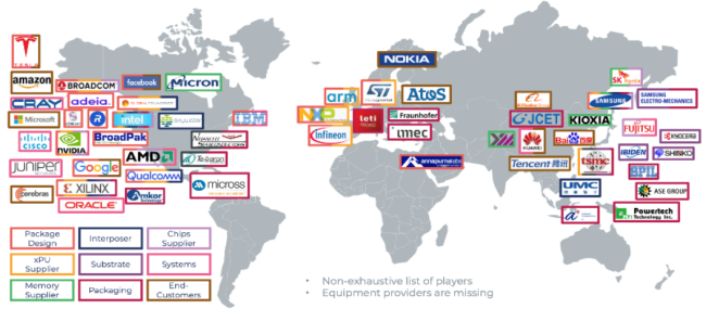
Global Semiconductor Advanced Packaging Market: Competitive Landscape
Currently, global participants in the advanced packaging industry can be broadly categorized into two groups.
The first group comprises companies with a wafer manufacturing background, such as TSMC, Samsung Electronics, and Intel. These firms focus on extending front-end process capabilities into advanced packaging, achieving system-level optimization through vertical integration. They typically view advanced packaging as a key technological lever to continue Moore’s Law, using it in synergy with wafer manufacturing to enhance overall performance and energy efficiency. For example, TSMC has developed the 3D Fabric advanced packaging platform, including CoWoS, SoIC, and InFO technologies, targeting high-end scenarios such as high-performance computing, high-bandwidth memory (HBM), and AI accelerators. CoWoS-S, for instance, enables integration with HBM and large-scale GPUs/SoCs, offering strong process synergy and customer customization capabilities.
The second group consists of OSATs (Outsourced Semiconductor Assembly & Test), such as ASE, JCET, and others. OSATs approach advanced packaging from an assembly–test–service perspective, emphasizing system-level packaging and scalable manufacturing. Their advantages lie in mature assembly/test process expertise, packaging materials and testing resources, and service networks close to end customers. Facing broad client demands, OSATs prioritize large-scale production, cost efficiency, and flexibility in back-end packaging. They possess rich experience in materials, assembly/testing processes, yield management, and logistics, making them well-suited for collaborations with multiple wafer fabs. These companies often adopt a “platform + customization” model, leveraging partnerships to access front-end wafers and back-end assembly/testing capabilities, and gradually advancing toward high-density interconnects and system-level packaging (e.g., FOCoS, XDFOI).
The table below summarizes the two types of participants and their roles in global advanced packaging:
Company Type | Advanced Packaging Focus & Key Features | Representative Companies |
Wafer Manufacturing | 1. Provide wafer-level silicon processing and advanced packaging, including multi-chip integration2. Offer end-to-end services in multi-chip integration | TSMC, Intel, Samsung Electronics, Shineway Microelectronics, etc. |
OSAT | 1. Transitioning from traditional packaging to advanced packaging, covering multiple technology types, strong cost control, quick response to demand2. Some focus on on-substrate (OS) multi-chip integration as a single segment | ASE, Amkor Technology, JCET, Tongfu Microelectronics, Huatian Technology, etc. |
The global advanced packaging market is highly concentrated, with outsourced manufacturing still dominant. According to Bosson Research, IDMs account for approximately 23% of the global advanced packaging market, wafer fabs for 12%, and independent OSATs for 65%. Market concentration is particularly pronounced among OSATs: in 2024, the top three players together held over 50% of the market, reflecting a clear “Matthew Effect.” As end-product demands diversify and packaging design complexity increases, R&D expenditures for IDM packaging continue to rise. Meanwhile, leading OSATs maintain the majority of the global advanced packaging market through their technological expertise and cost advantages.
Global Semiconductor Advanced Packaging Market: Market Segmentation Analysis
The research report includes specific segments by region (country), manufacturers, Type, and Application. Market segmentation creates subsets of a market based on product type, end-user or application, Geographic, and other factors. By understanding the market segments, the decision-maker can leverage this targeting in the product, sales, and marketing strategies. Market segments can power your product development cycles by informing how you create product offerings for different segments.
Key Company
ASE Technology Holding
Amkor Technology
Intel Corporation
TSMC
Samsung Electronics
JCET Group
Tongfu Microelectronics (TFME)
Powertech Technology Inc (PTI)
UTAC
Tianshui Huatian Microelectronics (Huatian)
SJ Semi
Hitech Semiconductor
China Resources Microelectronics
Chipmore Technology
Unimos Microelectronics
ChipMOS Technologies
King Yuan Electronics Corp (KYEC)
Nepes Corporation
WiseRoad
Forehope Electronic
China Wafer Level CSP
HANA Micron
Keyang Semiconductor
Payton Technologies
Forcera Materials
Biwin Storage
Walton Advanced Engineering
Kyocera
Chipbond
Market Segmentation (by Type)
Fan-Out
WLCSP
2.5D/3D
FCBGA
FCCSP
SiP
ED
Others
Market Segmentation (by Application)
Consumer Electronics
Healthcare
Industrial
Aerospace and Defense
Automotive
Other
Geographic Segmentation
North America
Europe
Asia-Pacific
South America
Middle East and Africa
Key Benefits of This Market Research:
• Industry drivers, restraints, and opportunities covered in the study
• Neutral perspective on the market performance
• Recent industry trends and developments
• Competitive landscape & strategies of key players
• Potential & niche segments and regions exhibiting promising growth covered
• Historical, current, and projected market size, in terms of value
• In-depth analysis of the Semiconductor Advanced Packaging Market
• Overview of the regional outlook of the Semiconductor Advanced Packaging Market:
Key Reasons to Buy this Report:
• Access to date statistics compiled by our researchers. These provide you with historical and forecast data, which is analyzed to tell you why your market is set to change
• This enables you to anticipate market changes to remain ahead of your competitors
• You will be able to copy data from the Excel spreadsheet straight into your marketing plans, business presentations, or other strategic documents
• The concise analysis, clear graph, and table format will enable you to pinpoint the information you require quickly
• Provision of market value (USD Billion) data for each segment and sub-segment
• Indicates the region and segment that is expected to witness the fastest growth as well as to dominate the market
• Analysis by geography highlighting the consumption of the product/service in the region as well as indicating the factors that are affecting the market within each region
• Competitive landscape which incorporates the market ranking of the major players, along with new service/product launches, partnerships, business expansions, and acquisitions in the past five years of companies profiled
• Extensive company profiles comprising of company overview, company insights, product benchmarking, and SWOT analysis for the major market players
• The current as well as the future market outlook of the industry concerning recent developments which involve growth opportunities and drivers as well as challenges and restraints of both emerging as well as developed regions
• Includes in-depth analysis of the market from various perspectives through Porter’s five forces analysis
• Provides insight into the market through Value Chain
• Market dynamics scenario, along with growth opportunities of the market in the years to come
• 6-month post-sales analyst support
Customization of the Report
In case of any queries or customization requirements, please connect with our sales team, who will ensure that your requirements are met.
Note: this report may need to undergo a final check or review and this could take about 48 hours.
Chapter Outline
Chapter 1 mainly introduces the statistical scope of the report, market division standards, and market research methods.
Chapter 2 is an executive summary of different market segments (by region, product type, application, etc), including the market size of each market segment, future development potential, and so on. It offers a high-level view of the current state of the Semiconductor Advanced Packaging Market and its likely evolution in the short to mid-term, and long term.
Chapter 3 makes a detailed analysis of the Market's Competitive Landscape of the market and provides the market share, capacity, output, price, latest development plan, merger, and acquisition information of the main manufacturers in the market.
Chapter 4 is the analysis of the whole market industrial chain, including the upstream and downstream of the industry, as well as Porter's five forces analysis.
Chapter 5 introduces the latest developments of the market, the driving factors and restrictive factors of the market, the challenges and risks faced by manufacturers in the industry, and the analysis of relevant policies in the industry.
Chapter 6 provides the analysis of various market segments according to product types, covering the market size and development potential of each market segment, to help readers find the blue ocean market in different market segments.
Chapter 7 provides the analysis of various market segments according to application, covering the market size and development potential of each market segment, to help readers find the blue ocean market in different downstream markets.
Chapter 8 provides a quantitative analysis of the market size and development potential of each region and its main countries and introduces the market development, future development prospects, market space, and capacity of each country in the world.
Chapter 9 details the production of products in major countries/regions and provides the production of major countries/regions.
Chapter 10 introduces the basic situation of the main companies in the market in detail, including product sales revenue, sales volume, price, gross profit margin, market share, product introduction, recent development, etc.
Chapter 11 provides a quantitative analysis of the market size and development potential of each region in the next five years.
Chapter 12 provides a quantitative analysis of the market size and development potential of each market segment (product type and application) in the next five years.
Chapter 13 is the main points and conclusions of the report.